skip to content

Semiconductor Physics Group


Self-assembled quantum dots

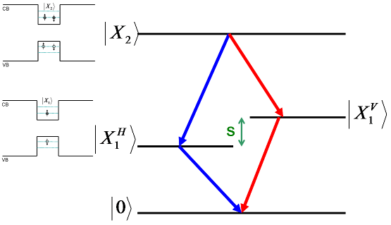
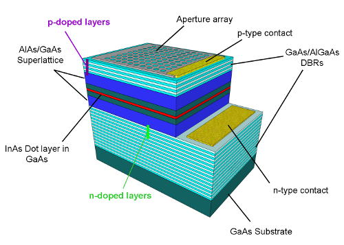
Electrons and holes confined withing a quantum dot (QD) present an interesting multi-level system (see figure 1) which can be used to investigate quantum phenomenon. Our work uses Stranski-Krastanov grown QDs, which are embedded within layed semiconductor structures grown via molecular beam epitaxy. Quantum light sources are made by placing optically active InAs QDs at the center of a AlGaAs/GaAs/AlGaAs quantum well sandwiched between two sets of Distrobuted Bragg Reflectors. Appriopriate doping is used to form a p-i-n diode structure, which allows electric field to be applied to the QDs. A diagram of a typical device is shown in figure 2.
Energy level diagram
Figure 1: Energy level diagram showing the ground (|0⟩), exciton (|X1⟩) and biexciton (|X2⟩) states. The ground state corresponds to when the QD is empty. As shown in the inset images, the exciton and biexciton states correspond to one or two electron hole pairs being confined inside the QD. The exciton state is split into two polarization dependent states labeled H and V. The separation between these polarization states (s) is known as the fine-structure splitting. Arrows show the possible photon-emitting decay paths from the biexciton state to the ground state.
p-i-n diode device structure
Figure 2: Diagram of the devices used in this project. A layer of QDs is placed at the center of a 2D GaAs quantum well which is sandwiched between AlAs/GaAs superlattice layers. The structure is between two sets of GaAs/AlGaAs distributed bragg reflectors (DBRs). Appropriately doped layers and two metal contacts allow electric field to be applied to the QDs. An opaque metal film is used to define apertures on the surface to allow small areas to be illuminated with a laser.


We perform quantum optics experiments to investigate the quantum properties of the carriers confined within a QD, with a view to developing applications in the field of quantum computation. In particular, we manipulate the energy levels of the QD via the application of external fields. The optically active nature of InAs QDs mean they can be used as an interface between flying photonic and stationary spin qubits; control of the energy eigenstates allows for the manipulation of the spin qubits when they are trapped within a QD. These factors, combined with the easily scalable nature of solid-state semiconductor materials, make QDs a very promising candidates for use in quantum computers.
Fine structure splitting
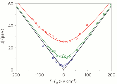
Figure 3: Graph of the magnitude of the fine-structure splitting (s) as a function of applied electric field. It is not possible to reduce s to zero, instead the two polarization states are observed to anticross. This is a signature of coherent coupling and indicates the hybridization of the two eigenstates.

Recent publications

For further information please contact: Matthew Pooley.