
Electron hole bilayers
Electron-hole bilayers
The sustained improvement in semiconductor growth techniques over the past 30 years has allowed electrons and holes to be confined in quasi two-dimensional systems.
An interesting and more complex possibility arises when electrons and holes are confined in two adjacent GaAs/AlGaAs quantum wells kept apart by a distance of few nanometres so that particle recombination is hindered by the presence of a
potential barrier. These systems are commonly known as electron-hole bilayers. The behaviour of the particles in such systems is the product of the relative contributions of inter-layer and intra-layer Coulomb interactions.

In particular, when the distance between the layers is comparable to the average separation between particles in the same layer, intriguing phenomena have been predicted to emerge that cannot be observed in an isolated layer, such as a supersolid Wigner crystal, an excitonic superfluid phase of indirect excitons with a BEC to BCS crossover. Condensation of excitons has been already observed in electron-electron and hole-hole bilayers at high perpendicular magnetic field, systems also known as quantum Hall bilayers. In the same spirit, electrically generated and independently contacted electron-hole bilayers have been intensively studied in the recent past, with a particular focus on transport measurements, such as Coulomb drag experiments (see below), which are used to probe directly the inter-layer interactions.
The most direct way (yet not the easiest) to induce a stable electron-hole bilayer is by electrical generation. A two-dimensional electron gas and a two dimensional hole gas are induced (by doping or field effect) at hetero-interfaces or in a double quantum well. Independently generated electron-hole bilayers have been already reported in the past: this approach is promising because it allows to study transport phenomena in electron-hole bilayers while keeping control of population densities in both layers.
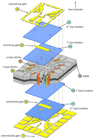 Fig.3 Schematic of the device | Here, we present ambipolar GaAs/AlGaAs devices, which can operate as both electron-hole and hole-hole bilayers. This flexibility has permitted, for the first time, to explore both the quantum Hall bilayer state and the zero-field electron-hole Coulomb drag in the same device. The inter-layer barriers (5 nm and 7.5 nm) of the double quantum well structure are the narrowest ever used in such systems. 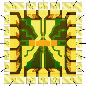 Fig.4 Picture of the electron-hole bilayer device after the fabrication process |
Modes of operation
The animation in Figure 5 explains how an electron-hole bilayer works. When no voltage is applied on any of the gates (in pale yellow), the Fermi level lies, naturally, between the bottom of the conduction band and the top of the valence band. In this situation, the electrons (or the holes) do not have enough energy to occupy the first states of the conduction band (or valence band for the holes).
Things change when a voltage starts to be applied on one of the gates (the top gate turns to yellow): the electric charge on the metal creates an electric field inside the structure, which modifies the energy profile of the bands. When the potential exceeds a certain threshold value, the Fermi level crosses the first quantised energy level of the closest quantum well, and the electrons start to populate the quantum well region, occupying a lateral region whose profile follows the gate shape (like a shadow). A similar situation occurs when the sign of the voltage is reversed: in this case, the Fermi level is moved downward, towards the edges of the valence band, and eventually crosses the top of the valence band to populate the quantum well closest to the gate with holes. It is natural, then, to inquire whether or not a combination of two biases would be sufficient to generate a bilayer: a population of electrons in the first well and one of holes in the second one. Unfortunately, there are a number of reasons why this cannot happen in a stable configuration. However, it is possible to kept the two layers at different electrochemical potential, by applying an external bias between the two wells. The external bias helps the Fermi level to move from the valence band in one layer to the conduction band in the well next to it, but the effective electric field across the barrier is low enough to avoid dielectric breakdown. | 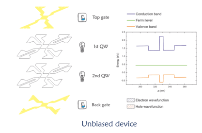 Fig. 5 Modes of operation of a bilayer device. |
The role of the interlayer bias
| An investigation has been conducted on the role of the inter-layer bias itself, aiming to understand how wave-function shape and position are modified by this. Figure Figure 6 a shows wave-function probabilities for constant densities of holes and electrons (4 x 1010 cm-2) when the inter-layer bias is varied. When the bias is increased, somewhat counter-intuitively, the wavefunctions are pushed towards the external walls of the wells. Actually, when the inter-layer bias increases, the voltages on the external gates must be reduced to keep the same densities: this reduces the band-bending in the structure and induces changes in thewavefunction shape, making the peaks closer together. | 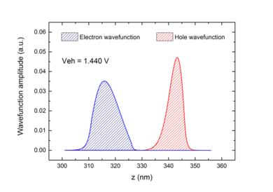 Fig.6 Distribution of the wavefunction probability |
Experiments
Electrical transport measurements of independently-contacted electron-hole bilayers can give us information about the state of the system. In particular, the inter-layer interactions between electrons and holes can be directly probed by means of the Coulomb drag technique. Coulomb drag is a process in which the interaction between electrons and holes in spatially separated conductors enables a current flowing in one layer to induce an open-circuit voltage in the other layer (see Figure 7). The drag resistance is defined as: Rdrag = Vdrag / Idrive | 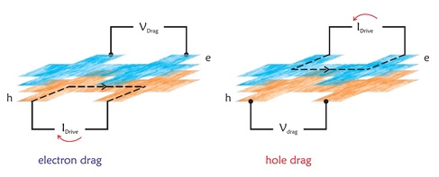 Fig.7 Schematic of a Coulomb drag experiment. An electrical current is passed through one layer: the carriers exchange momentum and energy with the particles of the other layer. Asa result, an open-loop voltage forms across the second layer. |
If one allows the contribution of inter-layer interactions to be expressed by a phenomenological scattering rate 1/τD, it is possible to demonstrate that Rdragα 1/τD, which makes the drag resistance a direct measurement of the interactions between the two layers.
Results
Coulomb drag measurements (see Figure 8) of electron-hole and hole-hole bilayers show unprecedented magnitude and allow one to compare the different effects of repulsive and attractive interactions in presence of the same background disorder. These measurements prove the fine quality of the devices and provide insights about the role of the charge density and the
thickness of the separating barrier.
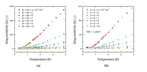
Fig.8 Drag resistivity as a function of temperature in a device with a 7.5 nm insulating barrier, when the device is operated in (a) hole-hole or (b) electron-hole configuration. Densities are varied in the range 4-10 x 1010 cm-2; in the electron-hole bilayer, full and empty dots correspond respectively to hole and electron drag, whereas, in the hole-hole bilayer, they correspond to top drag and back drag.
With the device in the hole-hole configuration, it was possible to study the bilayer in the quantum Hall bilayer regime (i.e. in a regime of strong perpendicular magnetic field). Low-temperature four-terminal measurements of the longitudinal and the Hall resistance of the two layers have been carried out in different configurations: results are reported in Figure 9.
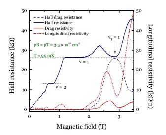 Fig.9 Hole-hole bilayer (hole densities pT = pB = 3.5 x 1010 cm-2 in a perpendicular magnetic | The current is passed in the top layer and Hall resistance and longitudinal resistivity are measured in both the drive and the drag layers. At low magnetic field (filling factor νT > 2 or equivalently B < 1.45 T) the traces corresponding to the drive layer follow the standard behaviour of a two dimensional gas, exhibiting well defined Hall plateaux and Shubnikov-de-Haas oscillations. In the same range of field, the drag signals (blue dash and red dot lines) are considerably small. However, when the system starts to approach the νT= 1 state (B = 2.9 T), the Hall drag resistance increases while, at the same time, the conventional Hall resistance in the drive layer decreases. Eventually, the two traces almost meet on a plateau at h/e2. At the same time the longitudinal and the drag resistance begin to increase, before suddenly dropping at a minimum value in correspondence to νT= 1. These observations have been interpreted as signs of formation of a magnetically-induced condensate of excitons. |
For more information
Croxall, A. F., K. Das Gupta, C. A. Nicoll, M. Thangaraj, H. E. Beere, I. Farrer, D. A. Ritchie, and M. Pepper.
"Anomalous coulomb drag in electron-hole bilayers." Physical review letters101, no. 24 (2008): 246801.
Zheng, B., A. F. Croxall, Joanna Waldie, K. Das Gupta, F. Sfigakis, Ian Farrer, Harvey Edward Beere, and David Alastair Ritchie.
"Switching between attractive and repulsive Coulomb-interaction-mediated drag in an ambipolar GaAs/AlGaAs bilayer device."
Applied Physics Letters108, no. 6 (2016): 062102.
Siciliani de Cumis, Ugo, Joanna Waldie, Andrew F. Croxall, Deepyanti Taneja, Justin Llandro, Ian Farrer, Harvey E. Beere, and David A. Ritchie.
"A complete laboratory for transport studies of electron-hole interactions in GaAs/AlGaAs ambipolar bilayers."
Applied Physics Letters110, no. 7 (2017):072105