Introduction to low-dimensional systems
- Introduction
- The GaAs/AlGaAs heterostructure and two-dimensional electron or hole system
- Split gates and one-dimensional electron gases
- References
Introduction
The two-dimensional electron gas (2DEG) formed in a GaAs-AlGaAs heterostructure is a very fruitful system for investigating quantum and interaction effects. Electrons are confined to a very narrow layer, becoming effectively two-dimensional. At low temperatures and with high-quality material, electrons can travel many microns without scattering off impurities, other electrons or phonons. Using lithographic techniques (such as split gates), it is thus possible to make structures through which electrons can travel without being scattered randomly, either elastically by impurities or inelastically by phonons or other electrons.
There have been many interesting developments and discoveries in this field of low-dimensional systems since 1986. The electron wavelength is often not much smaller than the channel width, so wires may act as waveguides, supporting only a few electronic modes (one-dimensional subbands). Very short ballistic channels (ones in which there is no scattering which causes a change in momentum) exhibit a quantised resistance h/ie2, where i is the number of 1D subbands occupied (van Wees et al, 1988, Wharam et al, 1988).
The GaAs/AlGaAs heterostructure and two-dimensional electron or hole systems
It is possible to confine electrons (or holes) in a two-dimensional (2D) layer (a 2D electron gas, called a 2DEG, or, for holes, a 2DHG) in a crystal, in such a way that they can move within that layer with minimal scattering. Such systems show quantum-mechanical properties such as the integer or fractional quantum Hall effects. Patterned gates above and below the 2DEG can be used to confine the electrons into narrow 1D or 0D regions, forming wires and dots, or to exclude electrons from a small region, forming an "antidot".
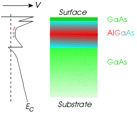
 Figure 1: Wafer cross-section and band structure.
Figure 1 shows a cross-section through a wafer consisting of layers of GaAs and AlGaAs. The wafer is grown by Molecular-Beam Epitaxy (MBE), which produces near-perfect crystalline layers of extreme purity, with nearly atomically sharp transitions between layers. To the left is shown the corresponding band diagram, i.e. the energy of the conduction band (the lowest energy electrons can have). The dashed line is the Fermi energy (roughly defined as the highest energy that electrons can have in equilibrium). The conduction bands of GaAs and AlGaAs are offset from each other, and this allows electron to collect in the GaAs but not in the AlGaAs. To provide the electrons, Silicon doping is included in the middle of the AlGaAs region (shown in red). These donors become positively ionised and provide electrons which collect in the neighbouring GaAs, though they cannot go too far away because they are attracted back to the positive ions. Thus they distort the conduction band into the shape shown, where there is a triangular "well" at the interface, and this goes slightly below the Fermi energy so that electrons can collect there. This well is so narrow that all the electrons there behave as quantum-mechanical waves, with the same wavefunction in the vertical direction. Thus the only degrees of freedom for the electrons are in the plane of the interface, and so they are effectively in a two-dimensional world.
When holes are used instead of electrons, acceptors are used instead of donors, and these become negatively charged. Holes (missing electrons in the valence band) then collect at the interface. The band diagram looks similar, but what is shown would be the valence band rather than the conduction band.
To constrain the electrons or holes still further, gates can be put on the surface, in what is called the split-gate technique.
Split gates and one-dimensional electron gases
The electrons in a 2DEG can be confined even further, becoming one or even zero dimensional (1D or 0D), by using metal Schottky gates on the surface of the wafer.
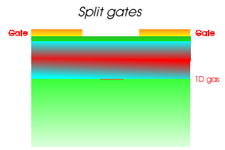
 Figure 2: Split-gate.
Figure 2 shows a cross-section through a wafer consisting of layers of GaAs and AlGaAs. With no surface gates, electrons are confined to the interface below the AlGaAs layer, forming a 2DEG. When a negative voltage is applied to the metal gates (shown in orange), electrons in the 2DEG beneath the gates are repelled, and eventually depleted altogether, leaving electrons only in a narrow strip between the two gates as shown. This is effectively a one-dimensional channel (called a 1D gas). This "split-gate technique" was pioneered by the Semiconductor Physics Group at the Cavendish Laboratory of the University of Cambridge, in England, in 1986, by Trevor Thornton and Professor Michael Pepper. Since then, it has been used by research groups all over the world to make low-dimensional devices. The surface gates can be patterned in almost any desired pattern.
References
D A Wharam, T J Thornton, R Newbury, M Pepper, H Ahmed, J E F Frost, D G Hasko, D C Peacock, D A Ritchie and G A C Jones, "One-dimensional transport and the quantisation of the ballistic resistance", J. Phys. C: Solid State Phys. 21, L209 (1988);
B J van Wees, H van Houten, C W J Beenakker, J G Williamson, L P Kouwenhoven, D van der Marel and C T Foxon, Phys. Rev. Lett. 60, 848 (1988).
T. J. Thornton, M. Pepper, H. Ahmed, D. Andrews, and G. J. Davies, Phys. Rev. Lett. 56, 1198 (1986).
