Surface Acoustic Waves (SAWs)
Introduction
Surface-acoustic waves (SAWs) are sound waves that travel parallel to the surface of an elastic material, with their displacement amplitude decaying into the material so that they are confined to within roughly one wavelength of the surface [1].
In a piezoelectric material such as gallium arsenide or quartz, the mechanical deformation associated with the SAW produces electric fields. To a good approximation, the electric fields do not affect the propagation of the mechanical wave, so the result is a variation in electrostatic potential that travels along with the SAW. Any thin layers of surface metal or conductive regions in the material affect the electrostatic potential variation around them, but the mechanical SAW propagates largely unaffected.
SAW transducers
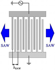
A SAW can be generated by applying a suitable oscillating signal to a suitably designed set of surface gates. A schematic diagram of a typical SAW transducer is shown below that consists of many pairs of interdigitated electrodes forming a grating-like structure, with the pitch of the transducer giving the SAW wavelength. By grounding one side of the transducer and applying a signal at a frequency given by the SAW velocity (roughly 2700 m/s for GaAs) divided by the pitch of the transducer, a SAW can be generated.
Electron-beam lithography allows sub-micrometre pitch transducers to be fabricated, enabling SAWs with frequencies in excess of 3 GHz to be generated on GaAs. Some pictures of SAW transducers are shown below.
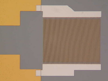
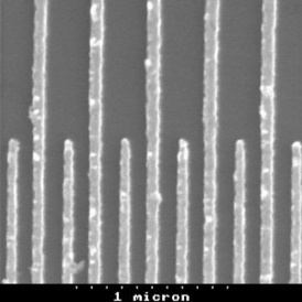
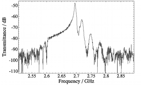
The reverse of the process used to generate SAWs can be used to detect them: when a SAW passes underneath a SAW transducer of the appropriate pitch, an alternating potential is generated across the transducer. A graph of the transmittance between two SAW transducers on GaAs, 4 mm apart, is shown below and exhibits a sharp peak corresponding to the generation of a SAW. Such a device can be used as a band-pass filter, and SAW devices are also used for convolvers and delay lines [1].
Wafers
The high-frequency single-electron-transport devices that have been fabricated to date used semiconductor wafers that contain a two-dimensional electron gas. The wafers consist of layers of GaAs and typically Al0.33Ga0.67As grown by molecular-beam epitaxy. The structure of a typical wafer is shown on the left below, and its calculated conduction band and electron wave-function is shown on the right. We see that the conduction-band offset between the two materials enables potential barriers to be formed, and by doping the wafer appropriately during the growth it is possible to bend the conduction bands so that a narrow potential well is formed that is below the chemical potential and populated with electrons. If the well is sufficiently narrow, and the electron density sufficiently low, then only the first sub-band in the confinement direction will be occupied. The result is an electron gas that is dynamically two-dimensional: the degree of freedom in the confinement direction is not accessible for reasonable electron energies.
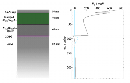
A wide variety of different wafer structures, with different materials, can be grown using molecular-beam epitaxy. Wafers can be grown that have more than one 2DEG in parallel, or with a hole gas, or with an empty quantum well, and n+ GaAs can be used to provide a gate within the wafer.
To make electrical contact to a 2DEG, a mixture of gold, germanium and nickel is deposited on the surface of the wafer and then heated so that it diffuses down into the wafer. This dopes the wafer very heavily so that it conducts, forming an Ohmic contact, and thin gold wires can be attached to the material on the surface.
To pattern a 2DEG, metal electrodes ("gates") can be deposited on the surface. When sufficient negative potential is applied to the gates, the conduction band beneath the gates can be raised so far that the energy of the lowest-lying state in the potential well is brought above the chemical potential and the 2DEG becomes depleted there. Alternatively, the 2DEG can be depleted by etching sufficiently far down into the doped layer of the wafer.
References
[1] See, for example, the books: "Surface acoustic wave devices and their signal processing applications," C. Campbell, Academic press, London, 1989. "Surface acoustic wave devices," S. Datta, Prentice-Hall, Englewood Cliffs, New Jersey, 1986. "Surface wave filters: design, construction and use", edited by Matthews, John Wiley and sons, New York, 1977.
