Low-temperature scanning probes
- Introduction
- Imaging quantum billiard orbits
- Erasable electrostatic lithography
- Coulomb charging in quantum dots
- Microconstrictions in long wires
- Backscattering from 1D channels
- Other experiments
Introduction
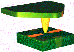
The scanning probe used in many of these experiments is a conductive atomic force microscope (AFM) tip. To generate topographic images the probe is configured as an AFM. A piezoresistive cantilever, which supports the tip, measures the force between the tip and the sample surface. To generate electrical images, such as conductance images, a bias is applied to the conductive tip which scans in a plane over the sample surface. The image contrast is then set by the device conductance.
Imaging quantum billiard orbits
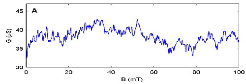
A quantum billiard is a large quantum dot where the electrons which are trapped inside travel in straight lines scattering only off the billiard’s boundary. Quantum billiards are classically mixed systems, exhibiting both regular and chaotic behaviour. Chaotic behaviour, where a small change in magnetic field strongly modifies conductance on an arbitrarily fine scale, is characterized by the presence of fractal conductance fluctuations. Classical behaviour is observed as periodic peaks in conductance as a function of magnetic field, called Aharonov-Bohm oscillations, which are understood to be the signature of regular stable closed-loop orbits with well defined areas. The amplitude of the associated wave functions, which are known as scarred wave functions, are concentrated along the underlying classical trajectories. A quantum billiard was fabricated using Erasable Electrostatic Lithography with dimensions 1.4 by 2.9 microns and a typical plot of conductance against magnetic field is provided below. Further analyses of this data shows that this quantum billiard is both chaotic and classical.
The tip then scanned 0.1 microns off the sample surface while the billiard conductance was recorded to generate the conductance image presented below as a 3D landscape. Analysis shows that the image is fractal over length scales from 0.1 to 1 micron demonstrating the chaotic nature. After high-pass filtering, the image revealed features common to scarred wave function demonstrating the classical nature.
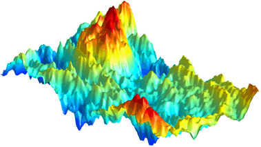
Future experiments will likely focus on smaller billiards where a one-to-one correspondance is expected with simulations and individual classical orbits can be resolved with high resolution.
[1] Imaging Fractal Conductance Fluctuations and Scarred Wave Functions in a Quantum Billiard R Crook, C G Smith, A C Graham, I Farrer, H E Beere, and D A Ritchie, Phys. Rev. Lett. 91 246803 (2003).
Erasable electrostatic lithography
Erasable Electrostatic Lithography (EEL) is a new lithographic technique for fabricating quantum devices such as quantum dots, 1D channels, and quantum billiards. For EEL a low-temperature scanning probe draws patterns of negative charge on a GaAs sample surface. The charge locally depletes electrons from a subsurface 2D electron system (2DES), so the charge pattern is projected onto an active layer to define electronic components for experiments investigating quantum phenomena. The charge patterns are stable for weeks, and the charge can be erased either locally using the scanning probe or globally by illuminating the sample with red light. EEL fabriction of a 1D channel is illustrated below, where the channel is defined by drawing lines of spots of charge.
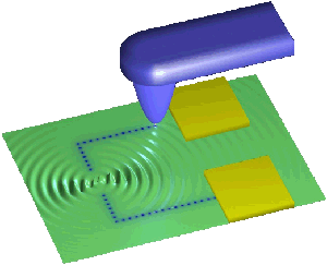
Once the 1D channel has been fabricated, it is characterised by positioning the tip 50 nm above the channel, then the tip bias is swept while the device conductance is recorded. The result is plotted below, where flat plateau in conductance demonstrate that an extremely high quality 1D channel has been fabricated. By drawing the component away from the surface electrodes, it is believed that disorder is reduced. A scanned gate microscopy image is used to locate the EEL component as presented in the inset.
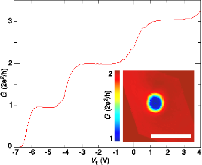
Quantum components can also be fabricated using existing techniques such as electron beam lithography or local anodic oxidation by AFM, but there are unique features of EEL which set it apart:
- Both lithography and measurement are performed in the same low-temperature high-vacuum environment. This reduces the measurement to lithography cycle time from weeks to hours, making EEL ideal for prototyping new designs and studying device geometry. If required, the previous design is globally erased without any need to warm up the cryostat.
- Components can be characterised and subsequently modified during the fabrication. This opens possibilities for dynamic fabrication, meaning the device is tuned to correct for inherent sample disorder as part of the fabrication. Tuning is achieved by drawing additional spots of negative charge or locally erasing charge with a probe biased positive. For example, the transmission of a 1D channel or the electrostatic barriers between quantum dots could by tuned during fabrication.
- Certain EEL quantum components have performance advantages compared to components fabricated using other lithographies. Defect compensation is a scheme to detect defect centres responsible for device noise, then draw a spot of charge to bring the noise source out of resonance. A similar scheme reduces the impact of background disorder to locally increase the electron mobility. Most quantum components are defined by applying a negative bias to patterned surface electrodes. The electrodes are necessarily metallic and subject to small voltage fluctuations from thermal noise. In contrast, EEL fabrication charges a necessarily insulating surface with fewer voltage fluctuations which may increase the electron phase decoherence time.
[1] Erasable Electrostatic Lithography for Quantum Components R Crook, A C Graham, C G Smith, I Farrer, H E Beere, and D A Ritchie, Nature 424 751 (2003).
Coulomb charging in quantum dots
The objective of this experiment was to control quantum dot electron-charging using a scanning probe.
The experiment is illustrated above where a charged probe is scanning over a sample. A 2DES forms at a GaAs/AlGaAs heterojunction 100 nm beneath the sample surface and biased sample surface electrodes define a 1D channel from the subsurface 2DES. By repeatedly scanning the probe to break up a parallel conducting layer, several quantum dots form in the proximity of the channel. The exact location of the dot depends upon the detailed sample disorder.
A small negative voltage is applied to the scanning probe, but the voltage is insufficiently negative to cause backscattering. As the probe scans, the probe electric potential controls the number of electrons in the quantum dots. Changes in dot electron occupancy cause an oscillation in the dot charge, which is detected by the nearby channel. Conductance images, like the one presented below, reveal sets of concentric halos centred over the dots.
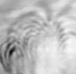
These two movies demonstrate that the images are sensitive to the tip bias, but not the channel characteristics. This proves that the quantum dots are located under the tip, outside the channel.
Sometimes the halo spacing changes at intersections between two sets of halos. This suggests that there is electrical interaction between the quantum dots.
[1] Quantum dot electron occupancy controlled by a charged scanning probe R Crook, C G Smith, W R Tribe, S O'Shea, M Y Simmons, and D A Ritchie, Phys. Rev. B 66 121301(R) (2002).
Microconstrictions in long wires
The objective of this experiment was to look for microconstrictions in long channels. The experiment is illustrated in Figure 1 where a charged probe is scanning over a sample. A 2DES forms 100 nm beneath the sample surface and biased sample surface electrodes define a long 1D channel from the 2DES. The channel is 4 microns long and 0.8 microns wide as shown in the scanning electron microscope image below.

There is ongoing debate as to whether a long channel, such as this one, is actually a long channel or just a series of short channels. Narrow portions of a long channel are called microconstrictions. When the probe is positioned over a microconstriction, it has more influence on the channel conductance. Therefore, by scanning over the channel with a negative voltage applied to the probe, the microconstrictions are revealed as changes in channel conductance. A typical conductance image is shown below, where the blue lines outline the actual location of the channel.
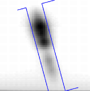
In this sample there are a series of 4 microconstrictions. Of course, other long channels may be different. By making further images with different tip biases, the conductance band edge along the length of the channel can be calculated. This is shown below.
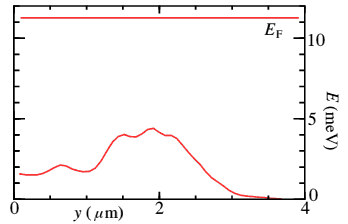
By applying a different bias to the two surface electrodes, the channel is shifted laterally by a few tens of microns. The microconstrictions change in magnitude, which suggests the disorder originates from the donor layer rather than the roughness of the surface electrodes.
Backscattering from 1D channels
The objective of this experiment was to scatter transport electrons off the potential perturbation generated by a biased tip. A 1D channel was used to detect backscattering.
The experiment is again illustrated in Figure 1, where a charged probe scans over a 2DES region adjacent to a 1D channel. Biased sample surface electrodes define the 1D channel from the subsurface 2DES.
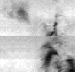
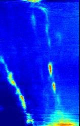
A large negative voltage is applied to the scanning probe. The electric field of the scanning probe forms a bump in the electric potential of the 2DES. Transport electrons travelling through the 2DES are scattered by the bump, which can also be considered as a mobile impurity. Electrons which travel trough the 1D channel, are scattered by the tip potential, and travel back through the 1D channel are detected as a change in channel conductance in a process known as backscattering. By scanning the probe, an image of channel conductance reveals the flux of backscattered electrons. Typical images are shown below where the channel is located just off the bottom right corner. Changing the number of transmissive 1D subbands has little effect on the images, which are dominated by disorder effects. These detailed images are intriguing. They are not yet fully understood.
[1] Imaging diffraction limited electronic collimation from a non-equilibrium 1D ballistic constriction R Crook, C G Smith, C H W Barnes, M Y Simmons, and D A Ritchie, J. Phys.: Condens. Matter 12 L167 (2000).
Other experiments
Scanning detectors
The objective of this experiment was to fabricate a channel on the corner of a chip, to make a scanning detector of electric potential. When a channel is biased in the tunnelling regime, the channel resistance is very sensitive to changes in the local electric potential. A channel was fabricated on the corner of a chip. The chip was inverted and mounted on a scan tube, to make a scanning detector. Images of the local potential were generated of a biased pattern of surface gates. A height resolution of 4 nm, a lateral resolution of 760 nm, and a sensitivity of 0.48 mV were achieved.
[1] Scanning noninvasive voltage probe operating at 4.2K A T Sellwood, C G Smith, E H Linfield, and M Y Simmons, Rev. Sci. Instrum. 72 2100 (2001).
Imaging cyclotron orbits
The objective of this experiment was to image electron cyclotron orbits in a weak magnetic field. The experiment is illustrated below where a probe is scanning over a sample with a subsurface 2DES. Surface electrodes define two channels separated by 4 microns. Electrons are injected through one channel, called the injection channel, and detected by the other, called the detection channel.
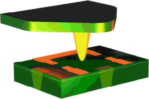
A large negative voltage is applied to the scanning probe. The electric field of the scanning probe forms a bump in the electric potential of the 2DES. This bump scatters electrons as they travel from the injection to the detection channel. By measuring the current through the detection channel, images are made of the path electrons take between the two channels. This is normally just a straight line.
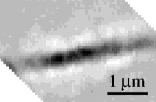
However, in a weak perpendicular magnetic field of 0.009 Tesla, the electrons follow a circular or cyclotron orbit.
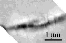
The cyclotron radius is measured from the image, and the electron energy calculated. Here the cyclotron radius is 10.3 microns, and the electron energy is calculated as 11.4 meV. Although the experiment is actually quite complicated, this is an amazing way to directly measure the electron energy.
The power of these images lie in the detail. Half way along the second image the path splits in two. This is the effect of background disorder in the 2DES potential, caused by the potential of ionised impurities. By comparing experimental images with computer simulations, it is feasible to determine the location and size of individual impurities.
[1] Imaging cyclotron orbits and small angle scattering sites in a high mobility two-dimensional electron gas R Crook, C G Smith, M Y Simmons, and D A Ritchie, Phys. Rev. B 62 5174 (2000).
1D wavefunctions
The objective of this experiment was to measure the electron density, which is related to the electron wavefunction, across a 1D channel.
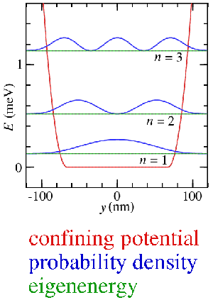
The above figure shows theoretical electron probability densities, and electron eigenenergies for the first three energy levels. Each energy level is called a 1D subband. The confining potential well has a flat bottom with parabolic sides, which is considered to be a good approximation to a 1D channel defined using surface electrodes. Each quantum state is called a 1D subband. The channel width and depth below the Fermi energy defines the number of 1D subbands which will be transmitted through the channel.
The experiment is illustrated in Figure 1 where a charged probe is positioned over a sample. A 2DES forms 100 nm beneath the sample surface and surface electrodes define a 1D channel from the 2DES. A small negative voltage is applied to the probe which visits a series of points across the width of the channel. At each point the width of the channel is swept from zero to four transmissive subbands. The width of the channel is controlled by the gate bias. The idea is that when the tip is positioned over a region of higher electron density, is has a larger influence over the channel conductance. Experimental results are presented below.
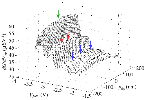
The x-axis is gate bias or channel width, the y-axis is probe position across the width of the channel, and the z-axis is the differential of the channel conductance. Peaks in conductance in the x-axis direction correspond to transitions between transmissive subbands. Superimposed on these peaks, now in the y-axis direction, are peaks which correspond to peaks in electron density. The first, second, and third subbands exhibit one, two, and three peaks in electron density, just as predicted by theory. Arrows have been added to make this clear. From the spacing between these experimental peaks, the energy spacing between 1D subbands can be calculated.
[1] One-dimensional probability density observed using scanned gate microscopy R Crook, C G Smith, M Y Simmons, and D A Ritchie, J. Phys.: Condens. Matter 12 L735 (2000).
Tip equipotentials
The objective of this experiment was to image the tip electric potential. The experiment is illustrated in Figure 1 above where a charged probe is scanning over a sample. A 2DES forms 100 nm beneath the sample surface and biased sample surface electrodes define a 1D channel from the 2DES. A large negative voltage is applied to the scanning probe. The electric field of the scanning probe forms a bump in the electric potential of the 2DES. This is illustrated below in a theoretical plot of electric potential against position.
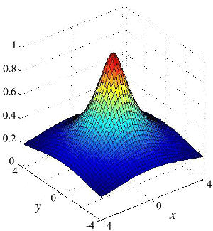
When the 1D channel is biased in the tunnelling regime, it's conductance is an extremely sensitive detector of the local electric potential. Therefore, by scanning the tip, 3D data can be collected about the tip electric potential. One slice of the 3D space is shown below, where the tip scans 30 nm above the sample surface.
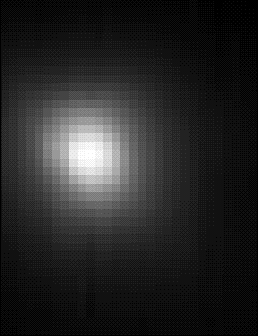
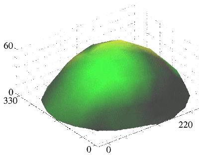
Three more images were made where the tip scanned 42 nm, 53 nm, and 65 nm above the sample surface. By combining all this data a surface of constant channel conductance can be calculated. A constant channel conductance corresponds to a constant electric potential, so an equipotential surface just below the end of the tip is obtained.
[1] Modification of 1D ballistic transport using an atomic force microscope R Crook, C G Smith, M Y Simmons, and D A Ritchie, Proceedings of the 24th International Conference on the Physics of Semiconductors, edited by David Gershoni, World Scientific Publishing 190 (1999).
